Flexible Electronic
Device Laboratory

The aim of our research group is to develop the high performance flexible and stretchable electronic systems using unusual classes of inorganic semiconductor materials in forms of nanoscale ribbons, nanomembrane, micro/nano-wires and one atomic layer film.

Currently, we are exploring integration methods including dry transfer techniques for patterning nanomaterials onto flexible substrates and ultra thin devices for the stretchable and conformal electronics.

Additionally, the strained engineered electronics would produce the ultra high performance for flexible devices. 

Our future picture is interesting opportunities for transparent and stretchable displays and sensitive electronic skins.

  • Stretchable high performance electronics
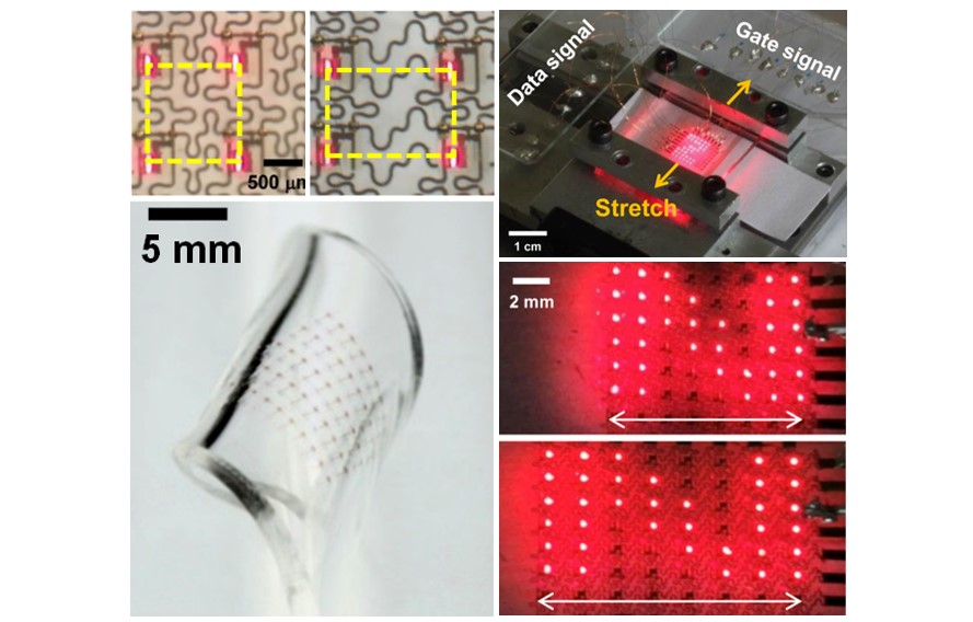
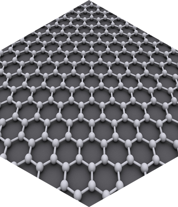
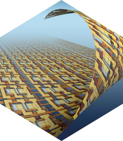
    Promising technologies for stretchable electronics that overcome the limitations of conventional electronics enable applications that are electronic skins, wearable electronic devices, stretchable displays, and electronics circuits. Using buckled graphene interconnects, our research group demonstrates stretchable Si logic devices that overcome the mechanical limitations such as poor stretchability and weakness to bending strain. The combination of Si and graphene can achieve both of good performance and stretchability
  • Ultrathin 2D material-based electronic skin application
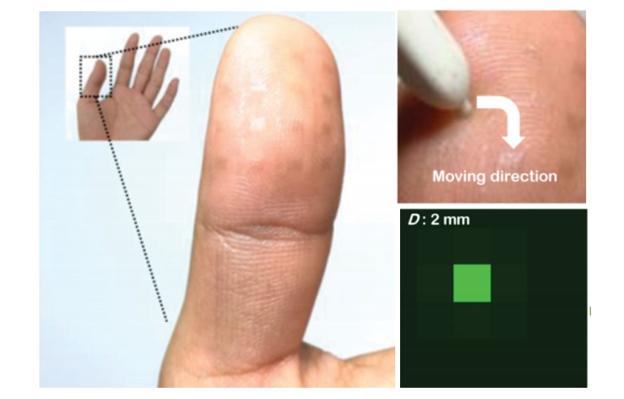
    One of the strategy for conformal devices is to make the device highly flexible and ultrathin. Highly flexible and ultrathin conformal devices on unconventional substrates have been researched for new applications that are healthcare monitoring systems, biotechnology, wearable electronics and e-skin
  • Two-dimensional materials in functional three-dimensional architectures with applications in photodetection and imaging
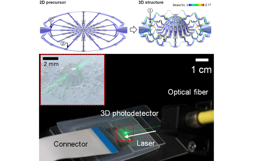
    Efficient and highly functional three-dimensional systems that are ubiquitous in biology suggest that similar design architectures could be useful in electronic and optoelectronic technologies. Here, we show that two-dimensional semiconductor/semi-metal materials can play critical roles in this context, through demonstrations of complex, mechanically assembled three-dimensional systems for light-imaging capabilities that can encompass measurements of the direction, intensity and angular divergence properties of incident light.
  • New approach of strain engineering for high performance devices
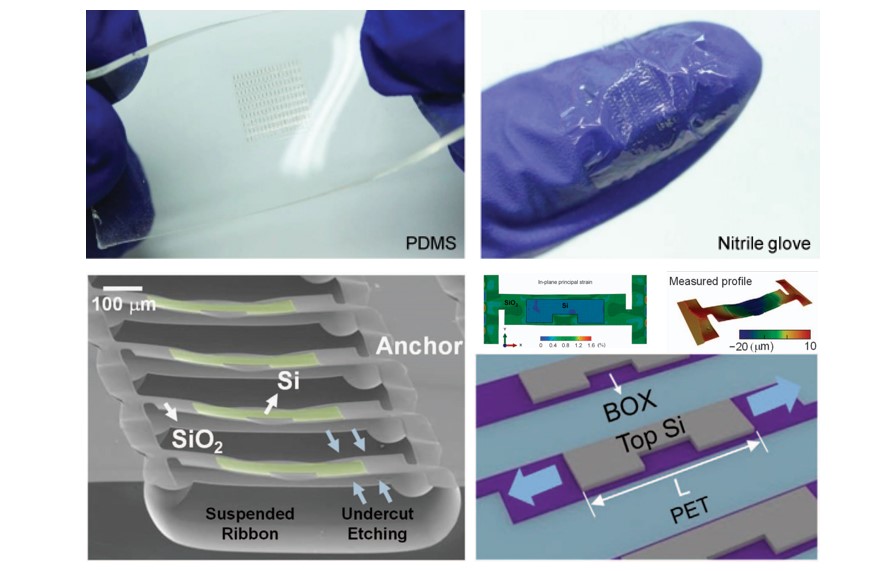
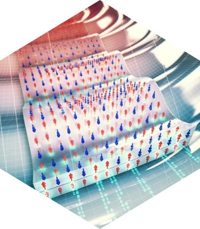
    Since the biaxial tensile strain applied to the Si channel reduced the inter-valley scattering and effective mass of electrons, the suspended and transferred Si TFTs showed a 19~40% increase in carrier mobility as compared with the unstrained devices on a bulk wafer.
PAPERS CITATIONS PATENTS H-INDEX
바 바 바 바